

I. Intro:
The Serial Peripheral Interface (SPI,發音類似spy) is a synchronous serial communication interface specification used for short-distance communication, primarily in embedded systems. The interface was developed by Motorola in the mid-1980s and has become a de facto standard (a custom or convention that has achieved a dominant position by public acceptance or market forces). Typical applications include Secure Digital cards (SD card) and liquid crystal displays (LCD). [1]
II. Character:
- Serial communication bus, with contrary to Parallel
- Master-Slave-Based, can have only one master and can have one or multiple slaves.
- Full duplex communication, send and receive simultaneously, both master and slave can transmit data at the same time.
- Synchronous communication, the data from the master or the slave is synchronized on the rising or falling clock edge.
- High speed, SPI > I2C > UART, SPI devices support much higher clock frequencies compared to I2C interfaces, typically up to a few MHz (so that is a few Mbps), so it is suitable for SDcard module.
- Short distance, around 20cm, UART > I2C > SPI.
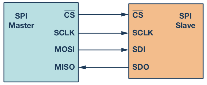
III. Interface:
- MISO:Master In, Slave Out 主入從出. Transmits data from the master to the slave.
- MOSI:Master Out, Slave In 主出從入. Transmits data from the slave to the master.
- SCK/ SCLK/ Clock:Serial Clock 串列時脈. The device that generates the clock signal is called the master.
- SS/ CS:Slave Select/Chip Select 從選. Active low, it is pulled high to disconnect the slave from the SPI bus. When multiple slaves are used, an individual chip select signal for each slave is required from the master. LOW表示裝置可以與Master通訊;HIGH表示不與Master通訊。只需普通的可輸出digital的pin, not restricted to arduino pin10,any digital pin is ok.
- SDO: Serial Data Out 串列資料輸出. An output signal on a device where data is sent out to another.
- SDI: Serial Data In 串列資料輸入.
IV. Data Transmission
To begin SPI communication, the master must send the clock signal and select the slave by enabling the CS signal. Usually chip select is an active low signal; hence, the master must send a logic 0 on this signal to select the slave. SPI is a full-duplex interface; both master and slave can send data at the same time via the MOSI and MISO lines respectively. During SPI communication, the data is simultaneously transmitted (shifted out serially onto the MOSI/SDO bus) and received (the data on the bus (MISO/SDI) is sampled or read in). The serial clock edge synchronizes the shifting and sampling of the data. The SPI interface provides the user with flexibility to select the rising or falling edge of the clock to sample and/or shift the data (see next section). Please refer to the device data sheet to determine the number of data bits transmitted using the SPI interface. [2]
![]()
![]()
V. Data Mode (Clock Polarity and Clock Phase)
The CPOL bit sets the polarity of the clock signal during the idle state.
The idle state is defined as the period when CS/SS is high.
The CPHA bit selects the clock phase. The rising or falling clock edge is used to sample and/or shift the data.
The master must select the clock polarity and clock phase, as per the requirement of the slave.
Depending on the CPOL and CPHA bit selection, four SPI modes are available.[2]
(Red lines denote clock leading edges, and blue lines, trailing edges.)[1]
b.t.w. 通常sample data的點會抓在那個bit方波的中間,因為頭尾不穩定![]()
![]()
VI. Multislave Configuration
- Regular SPI
An individual chip select for each slave is required from the master. Once the chip select signal is enabled (pulled low) by the master, the clock and data on the MOSI/MISO lines are available for the selected slave. If multiple chip select signals are enabled, the data on the MISO line is corrupted, as there is no way for the master to identify which slave is transmitting the data.[2]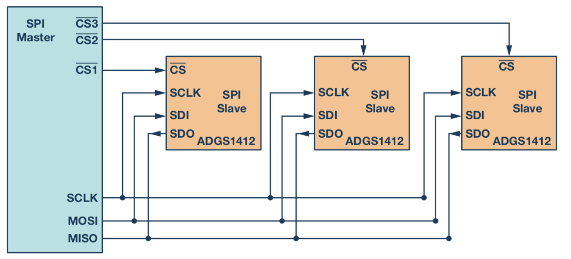
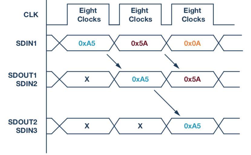
- Daisy-Chain
The chip select signal for all slaves is tied together and data propagates from one slave to the next. All slaves receive the same SPI clock at the same time. The data from the master is directly connected to the first slave and that slave provides data to the next slave and so on.
The number of clock cycles required to transmit data is proportional to the slave position in the daisy chain. For example, in an 8-bit system, 24 clock pulses are required for the data to be available on the 3rd slave, compared to only eight clock pulses in regular SPI mode. Daisy-chain mode is not necessarily supported by all SPI devices. Please refer to the product data sheet to confirm if daisy chain is available.[2]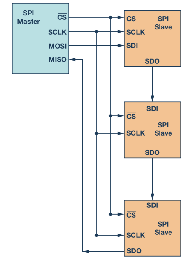
VII. Pros and cons
- Advantages [1]
- Full duplex communication in the default version of this protocol
- Push-pull drivers (as opposed to open drain) provide good signal integrity and high speed
- Higher throughput than I²C or SMBus. Not limited to any maximum clock speed, enabling potentially high speed
- Complete protocol flexibility for the bits transferred
- Not limited to 8-bit words
- Arbitrary choice of message size, content, and purpose
- Extremely simple hardware interfacing
- Typically lower power requirements than I²C or SMBus due to less circuitry (including pull up resistors)
- No arbitration or associated failure modes - unlike CAN-bus
- Slaves use the master's clock and do not need precision oscillators
- Slaves do not need a unique address – unlike I²C or GPIB or SCSI
- Transceivers are not needed - unlike CAN-bus
- Uses only four pins on IC packages, and wires in board layouts or connectors, much fewer than parallel interfaces
- At most one unique bus signal per device (chip select); all others are shared
- Signals are unidirectional allowing for easy galvanic isolation
- Simple software implementation
- Disadvantages [1]
- As the number of slaves increases, the number of chip select lines from the master increases. This can quickly add to the number of inputs and outputs needed from the master and limit the number of slaves that can be used. There are different techniques that can be used to increase the number of slaves in regular mode; for example, using a 3-to-8 demux/decoder to generate a chip select signal.
- Requires more pins on IC packages than I²C, even in the three-wire variant
- No in-band addressing; out-of-band chip select signals are required on shared buses
- Extensibility severely reduced when multiple slaves using different SPI Modes are required. Access is slowed down when master frequently needs to reinitialize in different modes.
- No hardware flow control by the slave (but the master can delay the next clock edge to slow the transfer rate)
- No hardware slave acknowledgment (the master could be transmitting to nowhere and not know it 可以不用有salve也可以傳)
- Typically supports only one master device (depends on device's hardware implementation)
- No error-checking protocol is defined
- Without a formal standard, validating conformance is not possible
- Only handles short distances compared to RS-232, RS-485, or CAN-bus. (Its distance can be extended with the use of transceivers like RS-422.)
- Opto-isolators in the signal path limit the clock speed for MISO transfer because of the added delays between clock and data
- Many existing variations, making it difficult to find development tools like host adapters that support those variations
- SPI does not support hot swapping (dynamically adding nodes).
- Interrupts must either be implemented with out-of-band signals or be faked by using periodic polling similarly to USB 1.1 and 2.0.
- Some variants like dual SPI, quad SPI, and three-wire serial buses defined below are half-duplex.
VIII. Demo: SPI LED Shift Register
Original experiment from: https://core-electronics.com.au/tutorials/arduino-workshop-for-beginners.html [4]
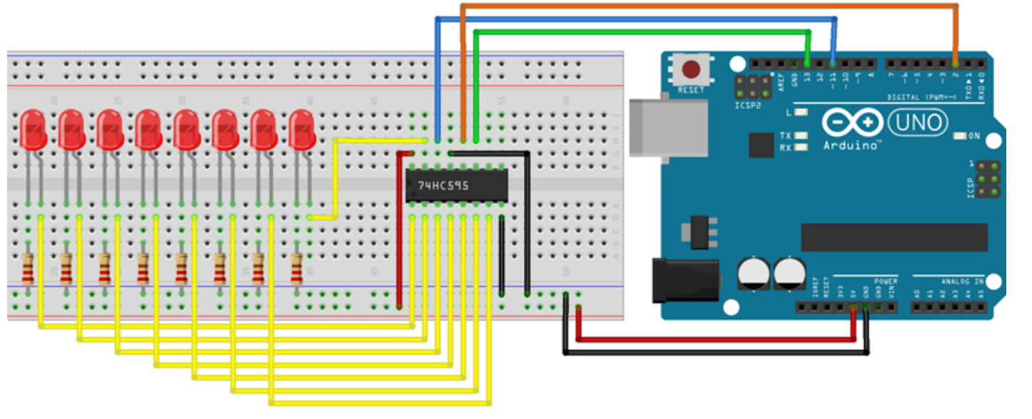
#include <SPI.h>

int slaveSelect = 2;

int delayTime = 50;

void setup() {
  pinMode(slaveSelect, OUTPUT);
  SPI.begin();
  SPI.setBitOrder(LSBFIRST);
}

void loop() {
  for (int i; i < 256; i++)
  //For loop to set data = 0 then increase it
  //by one for every iteration of the loop,
  //when the counter reaches the condition (256) it will be reset
  {
    digitalWrite(slaveSelect, LOW);
    //Write our Slave select low to enable
    //the SHift register to begin listening for data
    SPI.transfer(i);
    //Transfer the 8-bit value of data to shift register,
    //remembering that the least significant bit goes first
    digitalWrite(slaveSelect, HIGH);
    //Once the transfer is complete,
    //set the latch back to high to stop
    //the shift register listening for data
    delay(delayTime);  //Delay
  }
}
- 74HC595: "8-bit serial-in, serial or parallel-out shift register with output latches; 3-state."
https://www.arduino.cc/en/Tutorial/Foundations/ShiftOut - slaveSelect: can choose any digital pin, not restrict to pin10 on arduino
- SPI.setBitOrder: depend the slave device spec/datasheet. 像是頭先進還是尾巴先進
MSB (Most Significant Bit) Bit7, LSB (Least Significant Bit) Bit0 - SPI.setDataMode: depend the slave device spec/datasheet. Mode 0~3 as mentioned above.
- SPI.transfer: 可以傳int, hex, binary等等.
250//int, 0xFA//hex, B11111010//binary
Reference
[1] https://en.wikipedia.org/wiki/Serial_Peripheral_Interface
[2] https://www.analog.com/media/en/analog-dialogue/volume-52/number-3/introduction-to-spi-interface.pdf
[3] https://www.allaboutcircuits.com/technical-articles/spi-serial-peripheral-interface/
[4] https://www.youtube.com/watch?v=ZGaCXHvgcE4
[5] https://www.youtube.com/watch?v=fvOAbDMzoks
Read in markdown version: https://github.com/shannon112/Notes/blob/main/SPI/README.md
0 comments:
張貼留言
留言