

I. Intro:
The Inter-Integrated Circuit (I2C, pronounced I-squared-C) is a synchronous, multi-master, multi-slave, packet switched, single-ended, serial communication bus invented in 1982 by Philips Semiconductor (now NXP Semiconductors). It is widely used for attaching lower-speed peripheral ICs to processors and microcontrollers in short-distance, intra-board communication. Alternatively, I2C is spelled I2C (pronounced I-two-C) or IIC (pronounced I-I-C). Typical applications include GY series IMU and RTC clock module.[1]
II. Character:
- Serial communication bus, with contrary to Parallel
- Master-Slave-Based, multi-master, multi-slave.
- Half-Duplex communication, sharing one SDA line, can transmit and receive data, but not at the same time.
- Synchronous communication, the data from the master or the slave is synchronized on the clock edge.
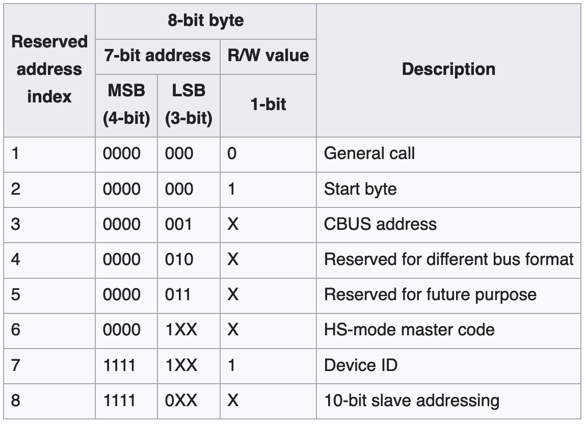
- Address, it can connect 128 (112) devices when using 7 bits addressing and up to almost 1024 (1008) devices when using 10 bits addressing. (There are a few reserved addresses such as 1111 XXX and 0000 XXX. So that 128-8-8=112.)
III. Interface:
- SDA:Serial Data 串列資料. Transmits data from the master to the slave or slave to the master.
- SCL:Serial Clock 串列時脈. Synchronize the data transfer between the devices on the I2C bus and it’s generated by the master device.
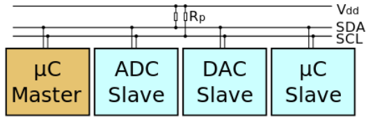
Since I2C is active low, if the two lines are “open-drain”, they need pull-up resistors such as 2K and 10K for 400kbps and 100kbps speed. Moreover, the Arduino Uno has pullup resistors built in that pull the SDA and SCK to 5 volts. An example schematic with one master (a microcontroller), three slave nodes (an ADC, a DAC, and a microcontroller), and pull-up resistors Rp is shown below.
IV. Speed
- Standard mode: 100 kbit/s (common I2C bus speed)
- Fast mode: 400 kbit/s (common I2C bus speed)
- Low-speed mode: 10 kbit/s, but arbitrarily low clock frequencies are also allowed.
Recent revisions of I2C can host more nodes and run at faster speeds (400 kbit/s Fast mode, 1 Mbit/s Fast mode plus, 3.4 Mbit/s High Speed mode, and 5 Mbit/s Ultra Fast-mode). These speeds are more widely used on embedded systems than on PCs.
V. Address
- 7-bit addressing
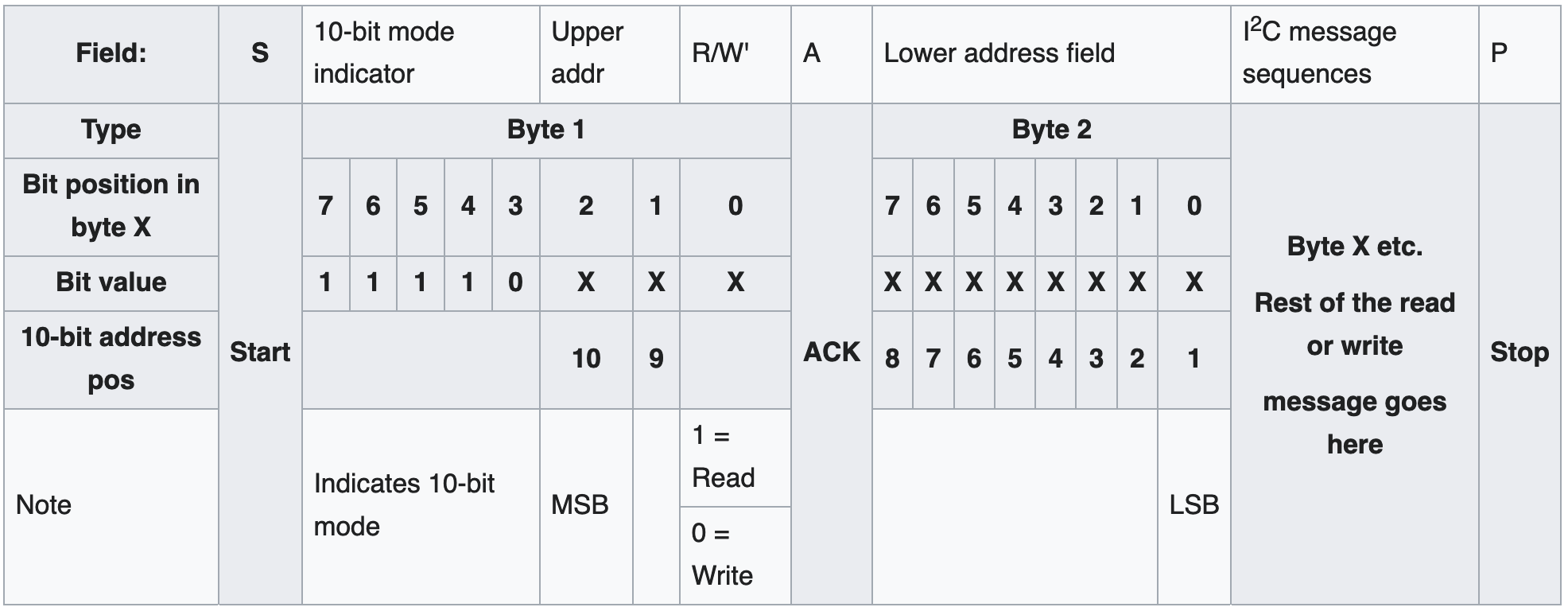
- 10-bit addressing
- Reserved addresses in 7-bit address space (保留)
- Non-reserved addresses in 7-bit address space (常見)
VI. Data Transmission
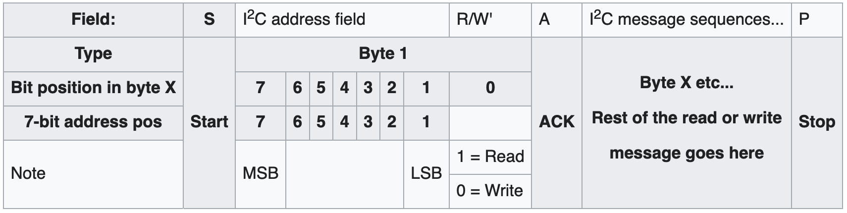
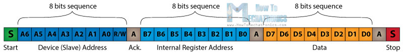
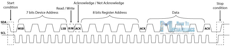
The data signal is transferred in sequences of 8 bits. The start condition occurs when data line drops low while the clock line is still high. After this the clock starts and each data bit is transferred during each clock pulse. The first 8 bits sequence which indicates the address of the slave (e.g. accelerometer ADXL345 in GY-80) to which the data is being sent. After each 8 bits sequence follows a bit called Acknowledge. After the first Acknowledge bit in most cases comes another addressing sequence but this time for the internal registers of the slave device (e.g. x-axis reading in ADXL345). Right after the addressing sequences follows the data sequences as many until the data is completely sent and it ends with a special stop condition.[2]
- The start condition occurs when data line drops low while the clock line is still high.
- The device addressing sequence stars with the most significant bit (MSB) first and ends with the least significant bit (LSB)
- The first 8 bits sequence composed of 7 bits address, and the 8th bit is used for indicating whether the master will write to the slave (logic low) or read from it (logic high).
- The next bit AKC/ NACK is used by the slave device to indicate whether it has successfully received the previous sequence of bits. The master device hands the control of the SDA line over to the slave device and if the slave device has successfully received the previous sequence it will pull the SDA line down, it is called Acknowledge. If the slave does not pull the SDA line down, the condition is called Not Acknowledge, and means that it didn’t successfully received the previous sequence which can be caused by several reasons. For example, the slave might be busy, might not understand the received data or command, cannot receive any more data and so on. In such a case the master device decides how it will proceed.
- The internal registers addressing: The internal registers are locations in the slave’s memory containing various information or data. For example the ADX345 Accelerometer has a unique device address and addition internal registers addresses for the X, Y and Z axis. So if we want to read the data of the X-axis, first we need to send the device address and then the particular internal register address for the X-axis. These addresses can be found from datasheet of the sensor.
- After the addressing, the data transfer sequences begin either from the master or the slave depending of the selected mode at the R/W bit. After the data is completely sent, the transfer will end with a stop condition which occurs when the SDA line goes from low to high while the SCL line is high.
VII. Pros and cons
- Advantages
- with clock, synchronous
- simple configuration in 2 wires, but up to hundreds of devices
- Disadvantages [1]
- Address management: The assignment of slave addresses is one weakness of I2C. Seven bits is too few to prevent address collisions between the many thousands of available devices. What alleviates the issue of address collisions between different vendors and also allows to connect to several identical devices is that manufacturers dedicate pins that can be used to set the slave address to one of a few address options per device. Two or three pins is typical, and with many devices, there are three or more wiring options per address pin.
- 10-bit I2C addresses are not yet widely used, and many host operating systems do not support them.
- Bus configuration: Automatic bus configuration is a related issue. A given address may be used by a number of different protocol-incompatible devices in various systems, and hardly any device types can be detected at runtime. For example, 0x51 may be used by a 24LC02 or 24C32 EEPROM, with incompatible addressing; or by a PCF8563 RTC, which cannot reliably be distinguished from either (without changing device state, which might not be allowed). The only reliable configuration mechanisms available to hosts involve out-of-band mechanisms such as tables provided by system firmware, which list the available devices. Again, this issue can partially be addressed by ARP in SMBus systems, especially when vendor and product identifiers are used; but that has not really caught on. The rev. 03 version of the I2C specification adds a device ID mechanism.
- Speed: I2C supports a limited range of speeds. Hosts supporting the multi-megabit speeds are rare. Support for the Fm+ 1 Mbit/s speed is more widespread, since its electronics are simple variants of what is used at lower speeds. Many devices do not support the 400 kbit/s speed (in part because SMBus does not yet support it). I2C nodes implemented in software (instead of dedicated hardware) may not even support the 100 kbit/s speed; so the whole range defined in the specification is rarely usable. All devices must at least partially support the highest speed used or they may spuriously detect their device address.
- Devices are allowed to stretch clock cycles to suit their particular needs, which can starve bandwidth needed by faster devices and increase latencies when talking to other device addresses. Bus capacitance also places a limit on the transfer speed, especially when current sources are not used to decrease signal rise times.
- Potential faults: Because I2C is a shared bus, there is the potential for any device to have a fault and hang the entire bus. For example, if any device holds the SDA or SCL line low, it prevents the master from sending START or STOP commands to reset the bus. Thus it is common for designs to include a reset signal that provides an external method of resetting the bus devices. However many devices do not have a dedicated reset pin, forcing the designer to put in circuitry to allow devices to be power-cycled if they need to be reset.
- Because of these limits (address management, bus configuration, potential faults, speed), few I2C bus segments have even a dozen devices. It is common for systems to have several such segments. One might be dedicated to use with high-speed devices, for low-latency power management. Another might be used to control a few devices where latency and throughput are not important issues; yet another segment might be used only to read EEPROM chips describing add-on cards (such as the SPD standard used with DRAM sticks).
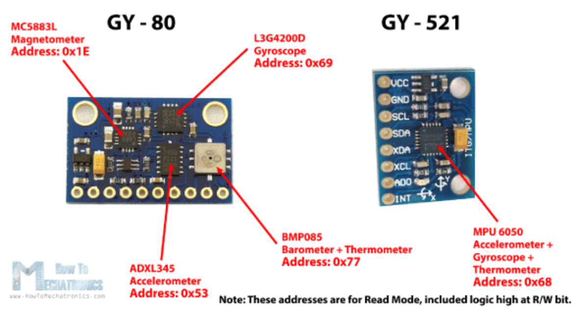
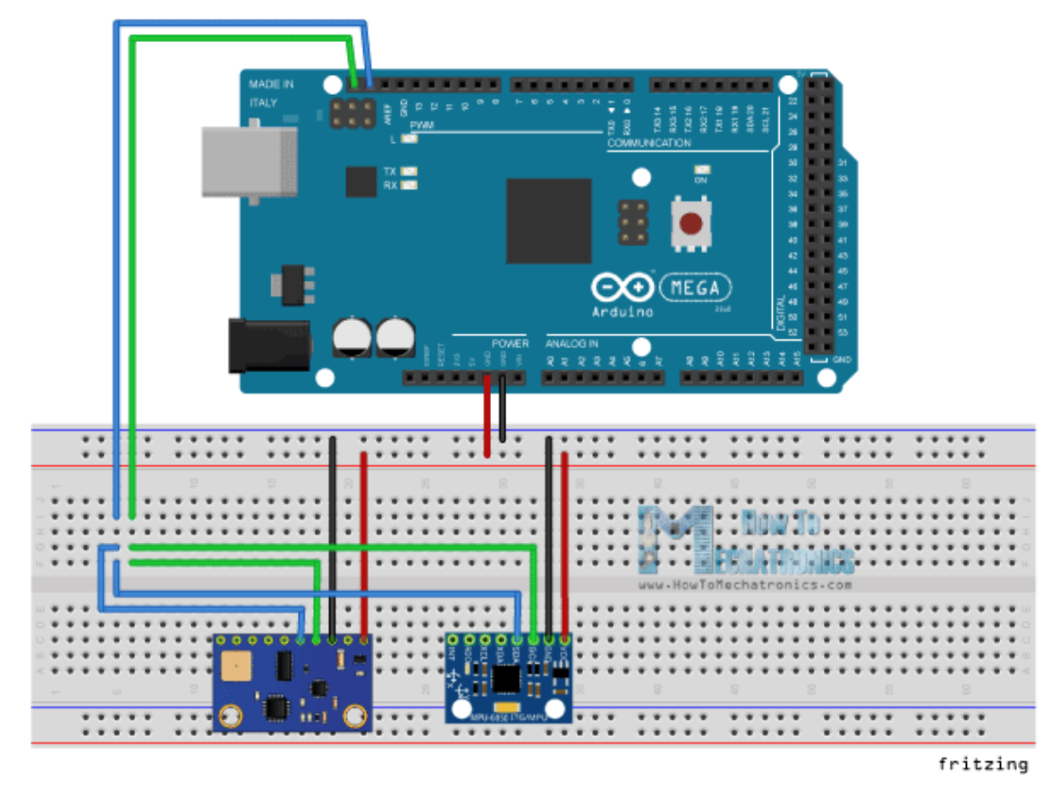
VIII. Demo: I2C GY-80 and GY-521 Reading
Original experiment from: https://howtomechatronics.com/tutorials/arduino/how-i2c-communication-works-and-how-to-use-it-with-arduino/ [2]
#include <Wire.h>

int ADXLAddress = 0x53; // Device address
#define X_Axis_Register_DATAX0 0x32 // Internal register addresses
#define X_Axis_Register_DATAX1 0x33 // Internal registers addresses
#define Power_Register 0x2D // Power Control Register

int X0,X1,X_out;
void setup() {
  // Initiate
  Wire.begin();
  Serial.begin(9600);
  delay(100);

  // Enable measurement
  Wire.beginTransmission(ADXLAddress);
  Wire.write(Power_Register);

  // Bit D3 High for measuring enable (0000 1000)
  Wire.write(8);
  Wire.endTransmission();
}

void loop() {
  // Begin transmission to the Sensor
  Wire.beginTransmission(ADXLAddress);
  //Ask the particular registers for data
  Wire.write(X_Axis_Register_DATAX0);
  Wire.write(X_Axis_Register_DATAX1);
  // Ends the transmission and transmits the data from the two registers
  Wire.endTransmission();
  // Request the transmitted two bytes from the two registers
  Wire.requestFrom(ADXLAddress,2);

  // Reads the data from the register
  if(Wire.available()<=2) {
    X0 = Wire.read();
    X1 = Wire.read();
  }

  // Print the raw data
  Serial.print("X0= ");
  Serial.print(X0);
  Serial.print(", X1= ");
  Serial.println(X1);
}
- GY-80 consists 5 different sensors and the GY-521 consists 3 different sensors. But there are only 5 device address.
- The device address and internal registers address can be found in datasheet.
- Or scan the device address: https://playground.arduino.cc/Main/I2cScanner/
- The device address included the 8th bit (read mode in this case)
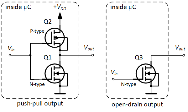
IX. Open Drain v.s. Push Pull
When you configure the GPIO pin of a microcontroller as Output. The Output pin can either be as Open-Drain type or Push-Pull Type. Both these configurations tell us how the GPIO pin of uC is designed internally. In most cases the push-pull type will be more advantageous than Open Drain Type. And modern MCUs have Push-Pull type [3]
- Open-Drain Type: There will be only one switch (transistor/MOSFET) inside the uC and this switch is connected to Ground and the other will be left floating.
- Push-Pull Type: There will be two switches (transistor/MOSFET) inside the uC and one switch will be connected to Ground and the other will be connected to Vcc/Vdd.
Reference
[1] https://en.wikipedia.org/wiki/I%C2%B2C
[2] https://www.youtube.com/watch?v=6IAkYpmA1DQ
[3] https://circuitdigest.com/forums/embedded/difference-between-open-drain-and-push-pull
Read in markdown version: https://github.com/shannon112/Notes/blob/main/I2C/README.md
It's remarkable. The way you describe the information is awesome. This will really help me out. Thanks for sharing.
回覆刪除Tableau Training in Chennai
Tableau Course in Chennai
Tableau Online Course
A brilliantly crafted piece that expertly combines deep technical knowledge with practical, real-world relevance. With outstanding clarity, rich detail, and highly actionable insights, it stands as a must-read resource for professionals dedicated to advancing their expertise in lighting design and modern innovation.
回覆刪除Integrated Circuits (ICs)